Memory is built from sequential chips. In this blog post, we’ll explore what sequential chips are, examples of them, and how they compose RAM.
Sequential Logic
In my post on boolean arithmetic and the ALU I completely ignored the issue of time. The ALU took input and spit out an output. The output was a function of the input. This is known as Combinatorial logic.
We want to be able to remember state. Physical time in the real world is continuous. We can’t mimic real time, but we can use discretization. This is like how we can use riemann sums to approximate the area under a function’s curve.
We can use a clock to turn physical time into discrete time. A clock is an oscillator of 0’s and 1’s at a fixed rate. Each cycle would be a digit time unit. Clock cycles are longer than the time it takes a bit to travel the distance from one chip in the architecture to another. This guarantees that by the time a sequential chip updates its state, the inputs will be valid.
Combinatorial: out[t] = function(in[t])
Sequential: out[t] = function(in[t-1])
Flip Flops
state[t] = function(state[t-1])
We now need a chip that can remember one bit of information from time t-1 so to use at time 1. There are two possible states, remembering t-1 or not remembering t-1 (1 or 0). Flipping between two possible states allows for this. Gates that can flip between two states are Flip-Flops.
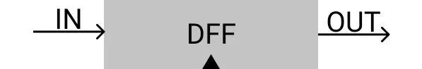
How is this done? Clocked Data Flip-Flops remember the data from the previous time unit it and output it in the current time unit. In the diagram, the triangle represents that the chip depends on time. The chip depends upon what happened in a previous state.
To remember a value forever until requested to load a new value we can use registers. If load(t-1) then out(t)=in(t-1) otherwise out(t)=out(t-1). Let’s take this 1-bit register as an example:
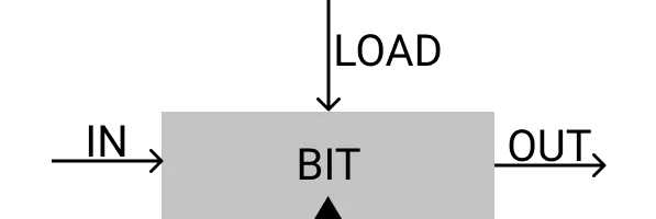
The implementation would consist of one MUX chip and one DFF chip. Once we have made a basic mechanism to remember a single bit over time, we can construct arbitrarily wide registers. To do this, we form an array of as many single-bit registers as needed, creating a register that holds multi-bit values.
Memory Units
Memory can be volatile or non-volatile. RAM is volatile while disk storage is non-volatile. The most elementary building block of RAM is the register. We can take a 1-bit registers and convert them into multi-bit registers. The width of a register, w (word width), usually ranges from 16-bit, 32-bit, 64-bit and so on.
When you stack registers together you can create RAM units. RAM as an abstraction is a sequence of n addressable registers with addresses of 0 to n-1. Also, at any time, we only select one register in RAM.
The width of the address input is equal to k. k is equal to log base 2 of n. For example, let’s say we have 16 registers. We need 4-bits to represent each register. 1111 would represent the last register’s address and 0000 would represent the first register’s address.
RAM is called “random access memory” because irrespective of the RAM size, we can access any register at the same time complexity - O(1).
Counters
Counters have 3 generic functions: reset to the first instruction, fetch the next instruction, and then fetch instruction n. The counter is a chip has realized these 3 primitive operations. Counters have 3 control bits load, inc, and reset to help with these operations. Let’s take a look at the HDL for a counter:
/**
 * A 16-bit counter with 3 control bits.
 * if      (reset[t]==1) out[t+1] = 0 (reset counter)
 * else if (load[t]==1)  out[t+1] = in[t] (set counter = value)
 * else if (inc[t]==1)   out[t+1] = out[t] + 1  (integer addition)
 * else                  out[t+1] = out[t] (counter does not change)
 */

CHIP PC {
    IN in[16],load,inc,reset;
    OUT out[16];

    PARTS:
	Inc16(in=oo,out=incd);

	Mux16(a=oo,b=incd,sel=inc,out=o);

	Mux16(a=o,b=in,sel=load,out=uu);

	Mux16(a=uu,b[0..15]=false,sel=reset,out=this);

	Register(in=this,load=true,out=out,out=oo);
}
Works Cited
- Nisan, Noam, and Shimon Schocken. The Elements of Computing Systems: Building a Modern Computer from First Principles. MIT, 2021.